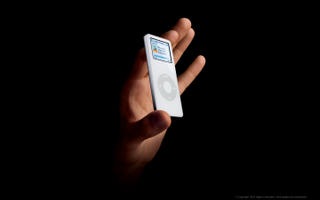
 I cried. I laughed and then was stuck by the Technology behind it. This review was one of its kind, for the latest iPod Nano. For long, I wondered what makes the iPod an iPod. I've broken open, Walkmans, TV Remote Controls, and Radios as I traced my quest as a budding electronics engineer. I've studied about the EEPROMs and RISC architecture.
But now, it was this review that gave me an insight on what went into the iPod Nano. Memory Chips, Processors and even the awesome thin stip of printed circuit behind the 'Click Wheel' caught me unaware. We had seen and wondered the beauty of the pencil-thick Nano. And now this insight review... We jus dont know, how far the technology can grow and what lies in our future.
Not withstanding the extreme review, Apple has admitted that there was some fault in Nano's LCD screen that made LCDs in some of the Nanos crack and break. However, Apple also maintained that it was a quality problem and not a design problem in Nano.
Even then, who wouldnt want to try their hands on the best tech gig the world has ever seen - 'iPod Nano'.
UPDATE: The Word Verification for comments is now turned 'ON' in this blog. Jus now, I removed three comment spams that sprang up jus minutes after we posted. Hope, at least the pain of typing the word for verification would turn down those spamming the blog. Keep Posting everyone. Cheers. Magnus.
5 comments:
Good information friend.
Apple is being in the forefront of the design-tech economy. I still remember when the first ever I-mac came out, a few months after there, there was a flood of rip-offs from China be it whole PC's or monitors that look like Imacs.
But did apple really manage to revolutionize tech as it is, or its just a revolution for the company. While there are many mp3 player makers out there flouting new designs by the day, what is the real sense or principle behind the Ipod Revolution to the community as a whole and to the future?
From a purely marketing standpoint, I wonder about Apple's decision to name this the Nano. What's their next model going to be called, the Pico? 10 years from now we'll probably be laughing at the size of the Nano and how little memory and features it has compared to then-current models. Methinks Apple should have at least waited until they had a model that uses actual nanotechnology before using that model name. :-)
I don't understand how technology works, so you must imagine how it boggles my mind to try to imagine circuit boards or whatever this small. How the heck can you manipulate something that small to ensure that all the connections are working? Do you use microscopic robotic arms? Live in the future brings up a good point. It's like what happened with 'giga' and 'mega.' Now where do you find a word that means "really really big"?
Circuits are build in places called Wafer Fabs. These are front-end production facilities where hundreds of chemicals are used to etch away the circuits that are 'drawn' with a quartz lense onto substrate coated silicon wafers. Certain chemicals are used at certain times to etch away certain part of the circuits. Normally there circuit are build in tiers, up to 7 tiers if im not mistaken. Thats 7 floors or circuits on-top of a micro small silicon chip. One silicon platter will have about 100-200 chips which is then cut into pieces with diamond cutters. About 60 to 70 % of the chips will work.
To view the ultra small circuits, they use very sensitive electron microscopes and laser scopes.
Heheh...i did internship in a wafer fab.
Post a Comment